NXS Hub — Datasheet
Project: NXS Hub Board: GMSL RECEIVER Design revision: V2.3 Document date: 2026-09-08 Document version: 1.1
1. Features
Section titled “1. Features”| Feature | Description |
|---|---|
| Dual GMSL3/2 deserialization | Two independent GMSL links → MIPI CSI-2 |
| MIPI CSI-2 output — Port A | 4-lane D-PHY, to FFC connector X3 |
| MIPI CSI-2 output — Port B | 4-lane D-PHY, to board-to-board X2 |
| Power-over-Coax (PoC) | Switched 12 V delivered to remote cameras over coax |
| Independent per-link power enable | GMSL A / GMSL B PoC individually switchable + protected |
| I²C level translation | 1.8 V core I²C ↔ 3.3 V system I²C, plus ERRB translation |
| I²C GPIO expander | Link enables, resets, PR_EN, INT, config |
| Control / trigger source mux | Select MCU vs external control of RX/TX/XTRIG lines |
| I²C source mux | Select FFC-side vs MCU-side I²C master |
| Level shifting / logic | ERRB status logic, FFC reset buffering |
| ESD protection | All CSI-2 lanes, GMSL SIO, and exposed I/O |
| Status indication | 3 status/error LEDs (incl. LOCK and ERRB) |
| Bring-up / debug | 10 test points on key rails and nets |
2. Applications
Section titled “2. Applications”- Embedded machine vision systems
- Robotics and autonomous platforms
- Multi-camera inspection systems
- Industrial vision integration platforms
3. Description
Section titled “3. Description”The NXS Hub is a dual-channel automotive camera aggregation / deserialization device. It receives high-speed serialized video and bidirectional control data from up to two GMSL (Gigabit Multimedia Serial Link) camera modules over coaxial cable, recovers the video streams, and forwards them to a host processor as MIPI CSI-2 data. The board also provides Power-over-Coax (PoC) to feed the remote cameras through the same coax used for data.
The core of the board is a Analog Devices / Maxim MAX96792A dual GMSL3/2
deserializer. It terminates two GMSL links (Link A and Link B) and maps their
received video onto two MIPI CSI-2 output controllers:
- CSI Port A (CSIA): 4 data lanes + 1 clock lane — routed to the FFC output connector
X3. - CSI Port B (CSIB): 4 data lanes + 1 clock lane — routed to the board-to-board connector
X2.
Camera control and configuration are handled over I²C with automatic 1.8 V ↔ 3.3 V level translation, an I²C GPIO expander for link/power enables and resets, and signal multiplexers that allow the deserializer’s control and trigger lines to be driven either by an on-carrier MCU or by an external header. Comprehensive ESD protection is fitted on every high-speed and exposed interface.
Primary signal flow:
GMSL Camera A ──coax──► X9 ──► MAX96792A (Link A) ──► CSI Port A ──► X3 (FFC, MIPI CSI-2)GMSL Camera B ──coax──► X8 ──► MAX96792A (Link B) ──► CSI Port B ──► X2 (board-to-board) ▲ I²C / control / reset / triggersPower flow:
12 V input (X1 / X4 / X5) ──► on-board regulators ──► 3.3 V, 1.8 V, 1.2 V, 1.0 V rails └──► high-side switch (TPS2H160A-Q1) ──► PoC 12 V ──► X9 / X8 (coax)Block diagram:
flowchart LR    subgraph CAM["GMSL Cameras"]        CA["Camera A"]        CB["Camera B"]    end
    X9["X9 — GMSL A coax"]    X8["X8 — GMSL B coax"]
    CA -- coax + PoC --> X9    CB -- coax + PoC --> X8
    subgraph BOARD["NXS Hub"]        U1["MAX96792A\nDual GMSL Deserializer"]        GPIO["I2C Expander"]        LVL["1.8V/3.3V xlate"]        I2CMUX["I2C mux"]        CMUX["ctrl/trigger mux"]        PoC["High-side PoC switch"]        PWR["Secondary power supply"]    end
    X9 --> U1    X8 --> U1    I2CMUX <--> X3["X3 — FFC MIPI CSI-2 (Port A)"]    I2CMUX <--> X2["X2 — B2B (Port B + control)"]    U1 <--> LVL    U1 --> X3    U1 --> X2    LVL <--> I2CMUX    CMUX <--> U1    PWR --> U1    PoC --> X9    PoC --> X8    GPIO<-->LVL    GPIO<-->PoC    GPIO<-->CMUX
    X1["X1 — 12V power in"] --> PWR    X4["X4 / X5 — 12V power in"] --> PWR    X6["X6 / X7 — EXT control"] --> CMUX
4. Absolute Maximum Ratings
Section titled “4. Absolute Maximum Ratings”Values below are per the cited component datasheets. Stresses beyond these ratings may cause permanent damage. These are stress ratings only; functional operation is not implied. Confirm against controlling datasheet revisions.
| Parameter | Symbol | Min | Max | Unit |
|---|---|---|---|---|
| 12 V power input | V(12V) | −0.3 | 20 | V |
| PoC output to coax | V(DC12_GMSL) | −0.3 | 20* | V |
| 3.3 V rail node | V(3V3) | −0.3 | 3.9 | V |
| 1.8 V rail node | V(1.8V) | −0.3 | 2.0 | V |
| 1.2 V rail node | V(1.2V) | −0.3 | 1.32 | V |
| 1.0 V rail node | V(1V) | −0.3 | 1.1 | V |
| MIPI CSI-2 lane pin | V(CSIx) | −0.3 | 1.32 | V |
| GMSL SIO pin | V(GMSL_x_SIO) | −0.3 | 2 | V |
| Operating junction temp | T_J | — | 150 | °C |
| Storage temperature | T_STG | −65 | 150 | °C |
*due to the system limitation
Section titled “*due to the system limitation”5. Recommended Operating Conditions
Section titled “5. Recommended Operating Conditions”| Parameter | Symbol | Min | Typ | Max | Unit |
|---|---|---|---|---|---|
| Main supply voltage | V(12V) | 4.7 | 12 | 17 | V |
| PoC output voltage | V(DC12_GMSL) | — | 12 | — | V |
| 3.3 V rail | V(3V3) | 3.20 | 3.30 | 3.40 | V |
| 1.8 V rail | V(1.8V) | 1.75 | 1.80 | 1.85 | V |
| 1.2 V rail | V(1.2V) | 1.17 | 1.20 | 1.23 | V |
| 1.0 V rail | V(1V) | 0.97 | 1.00 | 1.03 | V |
| Reference clock | f(REF) | — | 25 | — | MHz |
| I²C bus speed | f(SCL) | — | 400 | — | kHz |
| I²C High Level Voltage | Vh_I2C | — | 3.3 | — | V |
| GPIO High Level Voltage | Vh_IO | — | 1.8 | — | V |
| Ambient operating temp | T_A | −40 | +25 | +85 | °C |
| Operating PoC voltage range for GMSL video stream | V(12V) | 7 | 12 | 17 | V |
5.1 Power sequencing
Section titled “5.1 Power sequencing”Apply power in this order and remove it in the reverse order:
- Power up the host (the MIPI CSI-2 receiver, e.g. a Jetson).
- Power up the NXS Hub (12 V on X1 / X4 / X5).
Power down the NXS Hub first, the host last. A powered NXS Hub must never be connected to an unpowered host: the CSI-2 and control lines would drive the host’s unpowered I/O and back-power it through the protection diodes.
6. Interface Descriptions
Section titled “6. Interface Descriptions”6.1 GMSL Camera Inputs (Link A / Link B)
Section titled “6.1 GMSL Camera Inputs (Link A / Link B)”- Physical: Two coaxial connectors —
X9(GMSL A),X8(GMSL B), type2FA1-NZSP-PCBB6. - Function: GMSL3/2 serial link carrying forward video + reverse control, with PoC.
- Signals:
GMSL_A_SIO_P(X9),GMSL_B_SIO_P(X8), AC-coupled intoU1. - Protection: ESD + PoC filtering network per link.
6.2 MIPI CSI-2 Output — Port A (FFC)
Section titled “6.2 MIPI CSI-2 Output — Port A (FFC)”- Physical:
X3, 22+1 pos FFC/FPC (0545482272). - Cable: same-side (Type A) FFC, 22 positions, 0.5 mm pitch.
- Lanes:
CSIA_CLK±,CSIA_D0±…CSIA_D3±(4 data + 1 clock, D-PHY). - Sideband:
FFC_SCL,FFC_SDA(I²C),FFC_RESET_B,DC_3V3power out. - Role: Primary host video/data output.
6.3 MIPI CSI-2 Output — Port B + System Control (Board-to-Board)
Section titled “6.3 MIPI CSI-2 Output — Port B + System Control (Board-to-Board)”- Physical:
X2, 50+1 pos DF12 board-to-board (DF12NB-50DS-0.5V(51)). - Lanes:
CSIB_CLK±,CSIB_D0±…CSIB_D3±. - Control: deserializer RX/TX, resets, triggers (
DES_XTRIG0/1), enables, MCU-side I²C (MCU_SCL/SDA), mux selects,ERRB, config straps.
6.4 Control / Configuration Bus (I²C)
Section titled “6.4 Control / Configuration Bus (I²C)”-
System I²C (3.3 V):
DESER_SCL_3V3/DESER_SDA_3V3. -
I²C mux : selects between FFC-side (
FFC_SCL/SDA) and MCU-side (MCU_SCL/SDA) masters viaMUX_I2C_SEL. -
I2C MUX Truth Table :
| System Signal | MUX_I2C_SEL | Selected Source |
|---|---|---|
| DESERIALIZER I2C SDA | 0V | FFC_SDA |
| DESERIALIZER I2C SDA | 1.8V | MCU_SDA |
| DESERIALIZER I2C SCL | 0V | FFC_SCL |
| DESERIALIZER I2C SCL | 1.8V | MCU_SCL |
6.5 External Control Header
Section titled “6.5 External Control Header”-
Physical:
X6(0533980671) andX7(0532617006), 6+1 pos. -
Signals:
EXT_XVS0/DES_RX1,EXT_DES_TX1,EXT_XHS0/DES_RX2,EXT_DES_TX2,EXT_XTRIG0— routed through muxes (selected byMUX1_SEL,MUX2_SEL). -
Reset/Sync Truth Table :
| System Signal | MUX2_SEL | Selected Source |
|---|---|---|
| DESERIALIZER RESET | 0V | FFC_PIN_17 |
| DESERIALIZER RESET | 1.8V | MCU_RESET |
| DESERIALIZER XTRIG0 | 0V | EXT_XTRIG0 |
| DESERIALIZER XTRIG0 | 1.8V | MCU_XTRIG0 |
6.6 Power Input
Section titled “6.6 Power Input”- Physical:
X1(DF12 50+1),X4(0533980471),X5(0532617004). - Signal: 12 V + GND.
7. Connector Descriptions and Pinouts
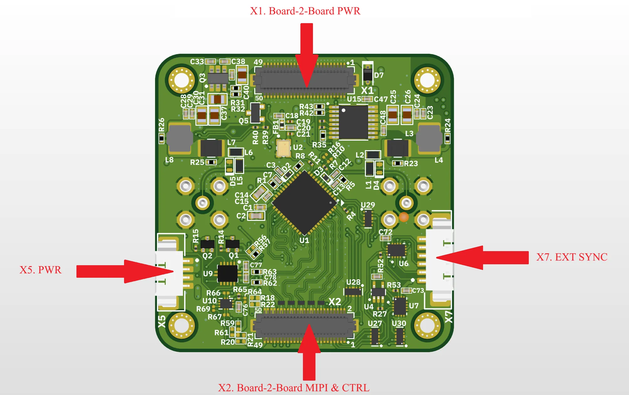
Section titled “7. Connector Descriptions and Pinouts”- Fig.1: Connectors location, top
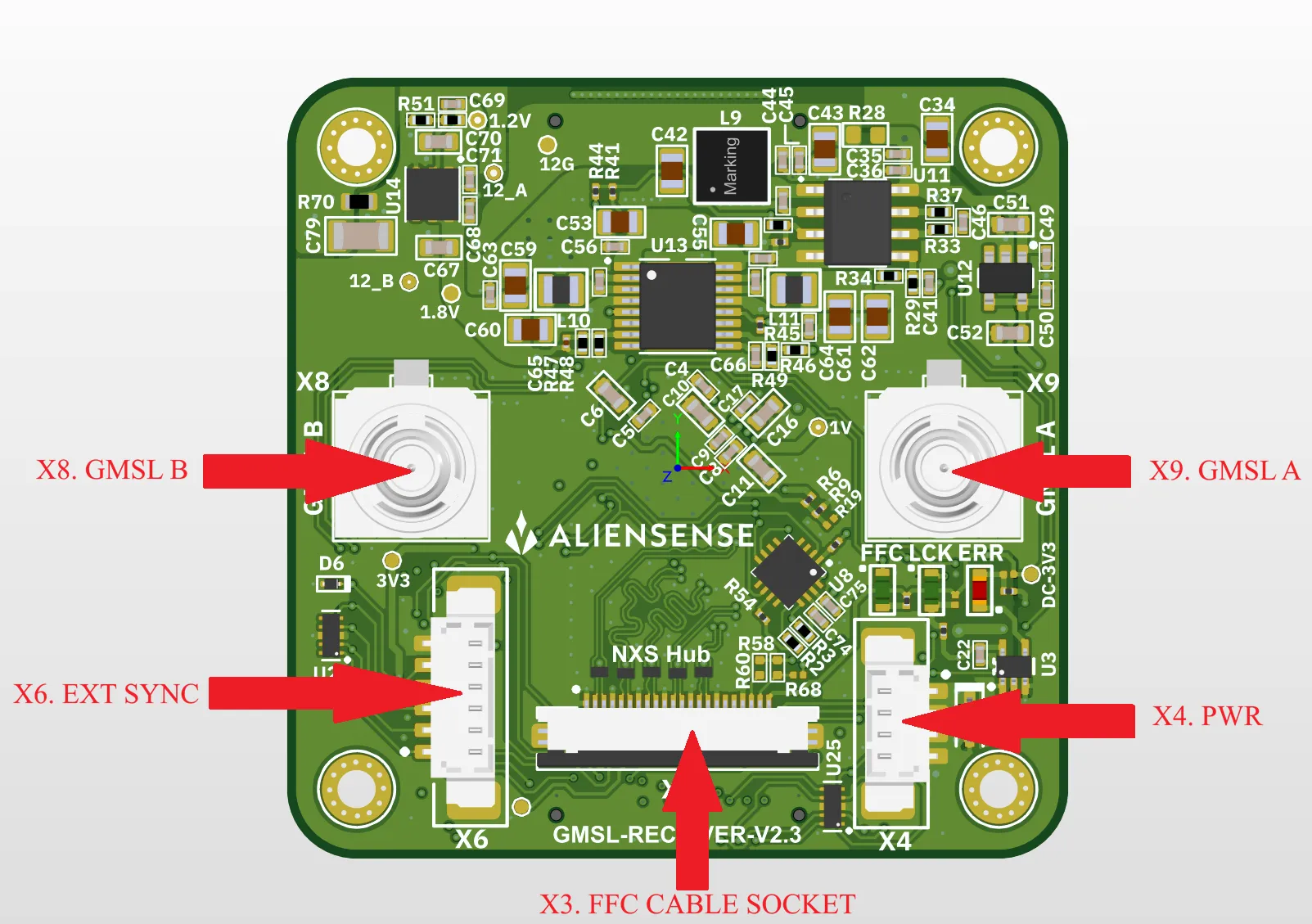
- Fig.2: Connectors location, bottom
7.1 X1 — 12 V Power Input (Board-to-Board)
Section titled “7.1 X1 — 12 V Power Input (Board-to-Board)”Part: DF12NB(5.0)-50DP-0.5V(51) · 50+1 positions
Odd pins = 12 V, even pins = GND, pin 51 = GND. (Pins 1–50 alternate 12V/GND.)
| Pin | Net | Pin | Net |
|---|---|---|---|
| 1,3,5…49 (odd) | 12V | 2,4,6…50 (even) | GND |
| 51 | GND |
7.2 X2 — Board-to-Board (CSI Port B + Control)
Section titled “7.2 X2 — Board-to-Board (CSI Port B + Control)”Part: DF12NB-50DS-0.5V(51) · 50+1 positions
| Pin | Net | Pin | Net |
|---|---|---|---|
| 1 | MUX1_SEL | 2 | DES_XTRIG0 |
| 3 | MUX2_SEL | 4 | DES_XTRIG1 |
| 5 | MCU_RESET | 6 | DES_TX1 |
| 7 | MCU_XTRIG0 | 8 | DES_PWDNB |
| 9 | GND | 10 | XVS0/DES_RX1 |
| 11 | DES_RESET | 12 | MUX_I2C_SEL |
| 13 | PR_EN_0 | 14 | CSIB_D3_N |
| 15 | GND | 16 | GND |
| 17 | XHS0/DES_RX2 | 18 | CSIB_D3_P |
| 19 | DES_TX2 | 20 | CSIB_D2_N |
| 21 | GND | 22 | GND |
| 23 | MCU_XHS0/DES_RX2 | 24 | CSIB_D2_P |
| 25 | MCU_DES_TX1 | 26 | CSIB_D1_N |
| 27 | MCU_DES_TX2 | 28 | GND |
| 29 | MCU_XVS0/DES_RX1 | 30 | CSIB_D1_P |
| 31 | GMSL_B_EN | 32 | CSIB_CLK_N |
| 33 | GMSL_A_EN | 34 | GND |
| 35 | SYS_EN | 36 | CSIB_CLK_P |
| 37 | MCU_SDA | 38 | CSIB_D0_N |
| 39 | MCU_SCL | 40 | GND |
| 41 | CFG1_R | 42 | CSIB_D0_P |
| 43 | ERRB_1V8 | 44 | reserved (factory configuration) |
| 45 | CFG0_R | 46 | reserved (factory configuration) |
| 47 | reserved (factory configuration) | 48 | reserved (factory configuration) |
| 49 | reserved (factory configuration) | 50 | reserved (factory configuration) |
| 51 | GND |
7.3 X3 — FFC / MIPI CSI-2 Output (Port A) — Primary Host Output
Section titled “7.3 X3 — FFC / MIPI CSI-2 Output (Port A) — Primary Host Output”Part: 0545482272 (Molex) · 22+1 positions
Cable: same-side (Type A) FFC only — see the §6.2 warning.
| Pin | Net | Description |
|---|---|---|
| 1 | GND | Ground |
| 2 | CSIA_D0_N | CSI-2 Data 0 − |
| 3 | CSIA_D0_P | CSI-2 Data 0 + |
| 4 | GND | Ground |
| 5 | CSIA_D1_N | CSI-2 Data 1 − |
| 6 | CSIA_D1_P | CSI-2 Data 1 + |
| 7 | GND | Ground |
| 8 | CSIA_CLK_N | CSI-2 Clock − |
| 9 | CSIA_CLK_P | CSI-2 Clock + |
| 10 | GND | Ground |
| 11 | CSIA_D2_N | CSI-2 Data 2 − |
| 12 | CSIA_D2_P | CSI-2 Data 2 + |
| 13 | GND | Ground |
| 14 | CSIA_D3_N | CSI-2 Data 3 − |
| 15 | CSIA_D3_P | CSI-2 Data 3 + |
| 16 | GND | Ground |
| 17 | FFC_RESET_B | Reset (buffered) |
| 18 | NetTP10_1 | Test/aux net (see TP10) |
| 19 | GND | Ground |
| 20 | FFC_SCL | I²C clock |
| 21 | FFC_SDA | I²C data |
| 22 | DC_3V3 | 3.3 V power out |
| 23 | GND | Ground (shield/tab) |
7.4 X4 / X5 — 12 V Power Input
Section titled “7.4 X4 / X5 — 12 V Power Input”Parts: X4 = 0533980471, X5 = 0532617004 (Molex) · 4+1 positions
| Pin | Net |
|---|---|
| 1 | 12V |
| 2 | 12V |
| 3 | GND |
| 4 | GND |
| 5 | GND |
7.5 X6 / X7 — External Control Header
Section titled “7.5 X6 / X7 — External Control Header”Parts: X6 = 0533980671, X7 = 0532617006 (Molex) · 6+1 positions
| Pin | Net |
|---|---|
| 1 | EXT_XVS0/DES_RX1 |
| 2 | EXT_DES_TX1 |
| 3 | EXT_XHS0/DES_RX2 |
| 4 | EXT_DES_TX2 |
| 5 | EXT_XTRIG0 |
| 6 | GND |
| 7 | GND |
7.6 X8 / X9 — GMSL Coaxial Camera Inputs
Section titled “7.6 X8 / X9 — GMSL Coaxial Camera Inputs”Part: 2FA1-NZSP-PCBB6 · coax (signal + shield)
| Connector | Pin 1 (signal) | Pin 2 (shield) | Link |
|---|---|---|---|
| X9 | GMSL_A_SIO_P | GND | GMSL A |
| X8 | GMSL_B_SIO_P | GND | GMSL B |
8. Indicators and Test Points
Section titled “8. Indicators and Test Points”8.1 Status LEDs
Section titled “8.1 Status LEDs”| Ref | COLOR | Function (from net context) |
|---|---|---|
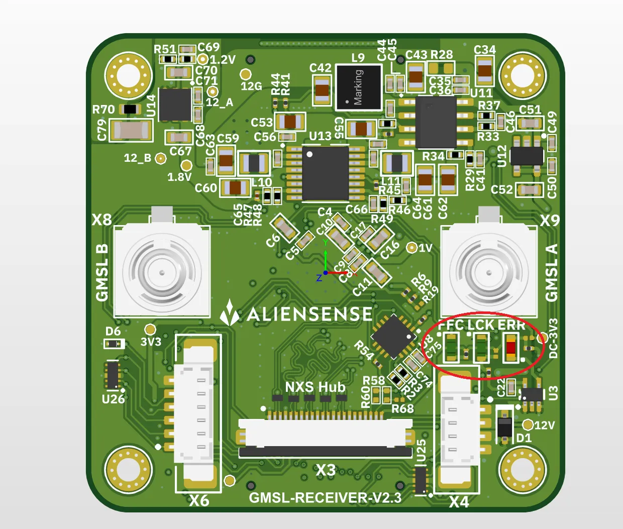
| LED1 | GREEN | Status (FFC cable connected) |
| LED2 | GREEN | Status (GMSL Link Locked) |
| LED3 | RED | Error / ERRB (GMSL Link Error) |
Fig.3: LED location
8.2 Test Points
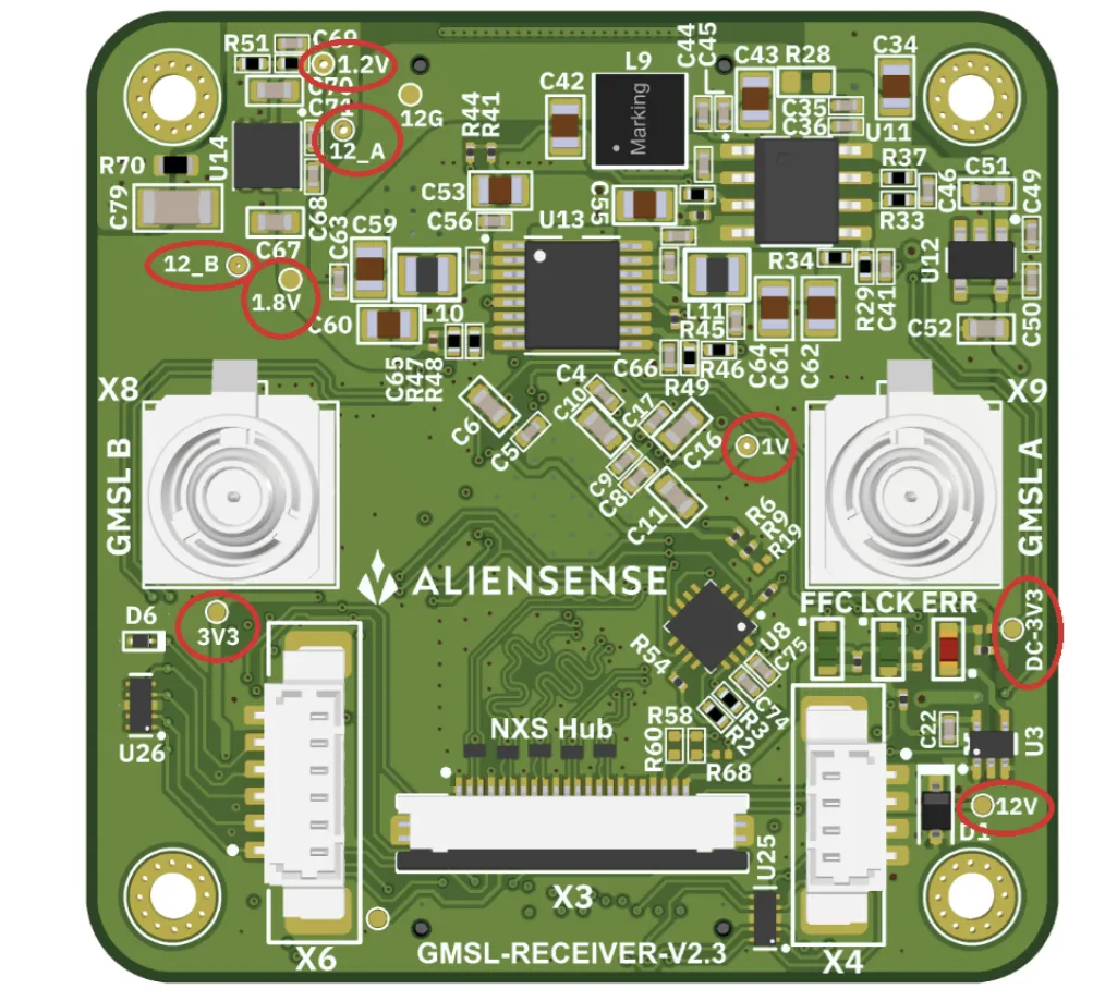
Section titled “8.2 Test Points”| Ref | Net / Label |
|---|---|
| TP1 | DC-3V3 |
| TP2 | 12V |
| TP3 | 12G (12 V ground/return) |
| TP4 | 12_A (GMSL A PoC) |
| TP5 | 12_B (GMSL B PoC) |
| TP6 | 3V3 |
| TP7 | 1.8V |
| TP8 | 1V |
| TP9 | 1.2V |
| TP10 | NetTP10_1 (aux, also on X3.18) |
Fig.4: Test points location
9. Mechanical Information
Section titled “9. Mechanical Information”Fig.5: GMSL Receiver board dimensions
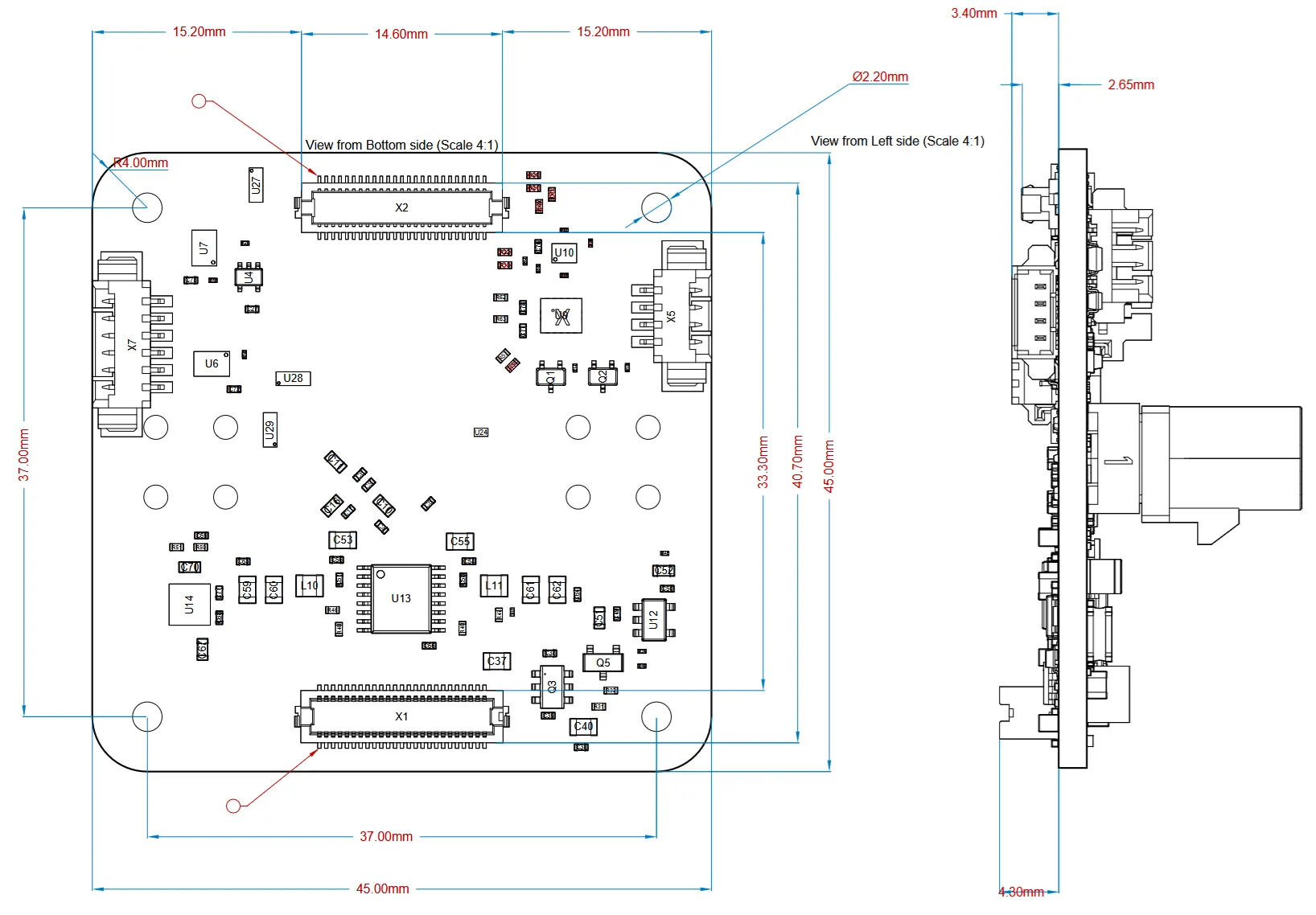
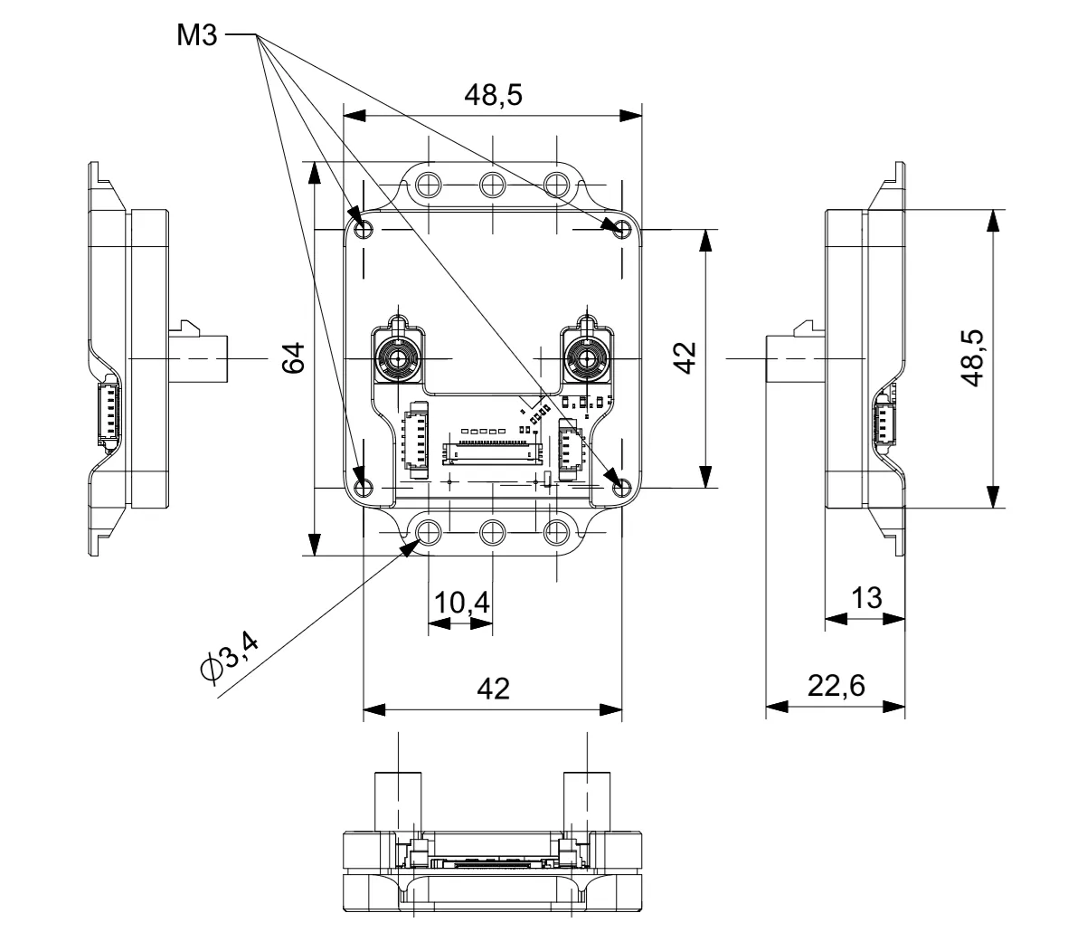
Fig.6: NXS Hub Dimensions
10. Cautionary Statement
Section titled “10. Cautionary Statement”Never hot-plug the camera or host connections. Cabling happens with both power supplies removed (§5.1), and power follows the §5.1 sequence — host up first, NXS Hub down first. The FFC output takes same-side (Type A) cables only (§6.2).
Safety instructions: see the Important Safety Instructions document on the product page.
Section titled “Safety instructions: see the Important Safety Instructions document on the product page.”11. Support
Section titled “11. Support”- Technical support: support@aliensense.com
- Documentation & downloads: product documentation and datasheets on the product page
- Aliensense · aliensense.com